
DDR3/DDR4/DDR5 Test Challenges
Double data rate (DDR) memory has progressed through four generations: improving in speed, efficiency, and memory capacity. The Joint Electron Device Engineering Council (JEDEC) released the fifth-generation double data rate (DDR5) synchronous dynamic random access memory (SDRAM) standard in July 2020. DDR5 will double the bandwidth in each dual in-line memory module (DIMM) over DDR4. DDR4 bandwidth ranges from 1.6 Gbps to a more recently attained 3.2 Gbps. DDR5 increases memory density to a potential maximum of 6.4 Gbps, doubling DDR4’s throughput frequency.
DDR5’s burst length is twice that of DDR4. Moreover, a DDR5 DIMM has two independent subchannels that improve memory controller scheduling and support concurrent operations. The same-bank refresh function of DDR5 enables a CPU core to use other DDR5 banks if one is already in use. DDR technology integrates error-correcting code (ECC) in-chip. (ECC finds and corrects errors before it sends data to the CPU.) DDR5 also lowers operating voltage by a small amount. Its modules will run at 1.1 V, compared with 1.2 V on DDR4. A lower operating voltage means better power efficiency, and the power saved adds up in large server farms.
A Small Inconvenience: New Slot
It appears DDR5 improves everywhere except for a small inconvenience in design and manufacturing. Both DDR4 and DDR5 modules have 288 pins and do not share the same pin layout. Thus, the DDR5 DIMM will need a new slot. However, like DDR4, DDR5 still uses a ball grid array (BGA) package and has the x4/x8 common footprint.
Though DDR5 offers far better performance than its predecessors, it has some testing challenges. A common signal integrity challenge found in DDR designs is timing issues with the memory controller. Historically, it was enough to run setup and hold time tests to verify data transfer. The speeds were slower, so margins were wider — meaning you had enough room to declare a DDR2 or DDR3 design within specification as long as you passed a setup and hold time test.
Eye Diagram Verification
However, with faster speed comes tighter margins. If you are working with DDR4 or DDR5, you no longer have enough margin to pass specifications with simple setup and hold time testing. Verifying DDR4 or DDR5 requires an eye diagram.
The DDR4 standard requires a specific margin and tolerances for random jitter and bit error rate within the specification. From this standard, you can create a mask in your oscilloscope. A mask defines a region on the oscilloscope’s display in which the waveform must remain to meet the requirements of your standard. If the eye closes too much and enters the mask, you likely have bit errors and will fail to meet the specification.
Test Challenges
DDR5 eyes start closing at the solder ball contacts of the DRAM package around 4 GT/s, depending on the signal integrity of the device under test. The DDR5 specification is defined at the solder balls of the DRAM because probing inside the chip package is exceptionally difficult to do in-system. Unfortunately, probing at the solder balls of the DRAM does not tell you if the eye is open or closed in the chip. Therefore, you must compensate with a decision feedback equalizer (DFE). A four-tap DFE, as described in the DDR5 specification, is necessary to remove the impulse response effects of the channel.
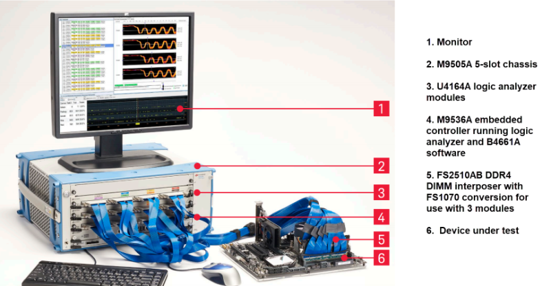
Apart from the signal integrity issues, you may encounter data corruption issues while validating a DDR4, LPDDR4, DDR5, or LPDDR5 design. Data corruption has a broad range of causes, typically signal integrity and functional issues. Oscilloscopes validate and debug the integrity of the signals, while logic analyzers debug and validate the functional or protocol compliance of memory systems.
Functional issues, where the memory devices do not receive the correct commands in the proper sequence or within specified timings, can result in data corruption and system crashes. Testing is essential to find these errors and their causes, whether physical or functional, so you can debug your design and prevent failures. You can use compliance test software to make testing and debugging easier.
DDR compliance test software runs on your oscilloscope to help validate the signal integrity and physical layer of your design. It automates the compliance test, verifies your design results, and generates a pass/fail report. All you need to do is connect the signals to your oscilloscope and run the application.
To test your design’s functional or protocol compliance, the right logic analyzer can capture all DDR signals simultaneously. For DDR5, protocol capture is possible with a logic analyzer at data rates up to 8,000 MT/s (when the column/address (CA) signals are operating at 4 GHz). Powerful analysis software decodes the memory protocol transactions and provides multiple views and graphs of the traffic flowing through the system. The views and graphs help validation engineers rapidly navigate the traffic flow to identify areas of concern. Protocol compliance validation software identifies exact issues in memory systems.
Oscilloscopes and compliance software can alleviate some of the challenges if you are working on the physical layer. Logic analyzers can help you test and debug your designs if you are working on functional and protocol compliance.
To learn more about the DDR memory test challenges, check out Keysight’s whitepaper DDR Memory Test Challenges: from DDR3 to DDR5.